


7.2.1 OPERATION OF THE DOMINO SAMPLING CHIP
The chip is realized in a 1.2 µm process[15] i.e. the minimal width of conducting lines and diffusion
areas of field effect transistors (FET's) is 1.2 µm. The circuit
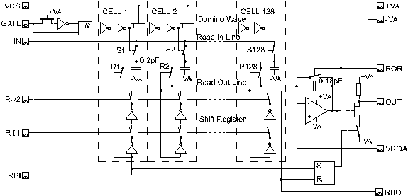
diagram of the DSC is shown in Fig. 7.1. The operation of the DSC consists of
the sampling phase and the readout phase.
 Figure
7.1:
Circuit diagram of the Domino Sampling Chip version 4 (DSC V4).
The principle of the sampling mechanism can be explained as follows: a logic
pulse is transmitted through two sequential CMOS inverters and therefore
reproduced; since the propagation time in an inverter is about 500 ps, the
pulse is delayed by 1 ns. Thus a signal propagating through a long chain
of inverters acts like a domino wave (see Fig. 7.2). A positive edge applied at
the GATE pad starts the domino wave which after every second inverter connects
the read-in line with a capacitor, thus sampling an storing the instantaneous
level of the read-in line voltage.
Figure
7.1:
Circuit diagram of the Domino Sampling Chip version 4 (DSC V4).
The principle of the sampling mechanism can be explained as follows: a logic
pulse is transmitted through two sequential CMOS inverters and therefore
reproduced; since the propagation time in an inverter is about 500 ps, the
pulse is delayed by 1 ns. Thus a signal propagating through a long chain
of inverters acts like a domino wave (see Fig. 7.2). A positive edge applied at
the GATE pad starts the domino wave which after every second inverter connects
the read-in line with a capacitor, thus sampling an storing the instantaneous
level of the read-in line voltage.
 Figure
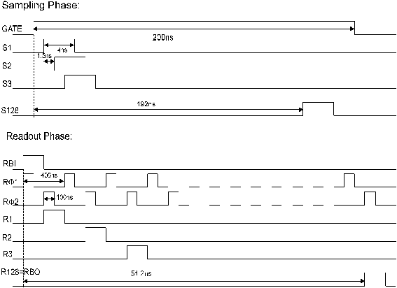
7.2:
Control signals for operating the DSC. The signals S1,...,S128, and R1,...,R128
are internal signals of the DSC (Fig. 7.1). The delays of the sampling phase
depend on the sampling frequency; the indicated values are calculated for a
sampling frequency of 667 MHz.
The speed of the sampling mechanism is controlled by the domino speed voltage
VDS (Fig. 7.1), which influences the propagation time of the domino
wave. For values of 1 V< VDS <5 V sampling frequencies between 100
and 800 MHz are obtained.
Figure
7.2:
Control signals for operating the DSC. The signals S1,...,S128, and R1,...,R128
are internal signals of the DSC (Fig. 7.1). The delays of the sampling phase
depend on the sampling frequency; the indicated values are calculated for a
sampling frequency of 667 MHz.
The speed of the sampling mechanism is controlled by the domino speed voltage
VDS (Fig. 7.1), which influences the propagation time of the domino
wave. For values of 1 V< VDS <5 V sampling frequencies between 100
and 800 MHz are obtained.
The read out of the stored information is started by applying the RBI (read bit
in) pulse, which is clocked through the read-out shift register with the
signals R f 1, R f 2 . One clock cycle, consisting of
a non-overlapping R f 1-pulse and R f 2-pulse of
100 ns each, has a duration of 400 ns (Fig. 7.2). Starting with the
R f 2-pulse the corresponding capacitor is connected over the
read-out line to a charge-sensitive output amplifier.
The ROR-pulse (read-out reset pulse) resets the amplifier in phase with the
R f 1-pulse. At the 128th clock cycle, the RBO (read
bit out) pulse appears at the end of the shift register, indicating the
successful read-out of the chip. This pulse disconnects the output of the
amplifier from the output pad, thus enabling the serial read-out of several
DSCs connected to the same output line. The RBO-pulse can be used as a RBI for
the next chip in the chain. The present read-out frequency is 2.5 MHz per
bin, which corresponds to 51.2 µs for one DSC.
[15] The chip is fabricated by FASELEC AG.