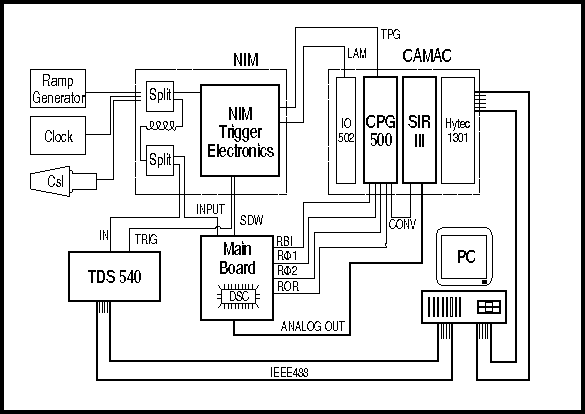
Fig. 3: Block Diagramm of the DSC test setup.
The universal programmable clocked pattern generator CPG500 has an 8K memory, its 8Bit databus is accessible from front-panel lemo connectors. The clock frequency is externally supplied and is at most 25MHz. In addition, the CPG500 is capable of conditional branching triggered by an external pulse, e.g. jumping into a subroutine if programmed so. The downloading of the CPG500 code, the code for the 8X305 processor of the SIROCCO III as well as the read-out of the SIROCCO III is done using a HYTEC 1331 CAMAC-PC interface and a PC. The digital scope TDS540 is controlled over an IEEE488 bus with the PC. The chip is operated in the trigger mode; i.e. after the splitting of the analog signal, one part is delayed and connected to the DSC and the digital scope, whereas the other part is fed into the NIM electronics to generate the trigger signals (Fig. 3): Immediately, the SDW signal starts the domino wave in the DSC and the TRIG signal enables the digital scope to store the analog pulse. After ~5 musec the CPG500 is triggered by the TPG (trigger pattern generator) pulse to provide the readout signals (RBI, RP1, RP2, ROR) for the DSC and the CONVERT signal for the SIROCCO III. After the readout phase, which takes about 100 musec, the LAM signal for the data acquisition is generated, thus pointing at valid data in the SIROCCO III and the digital scope.
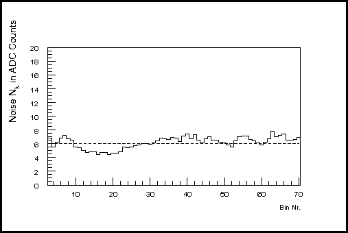
Fig. 4 shows the noise in 70 bins of the DSC, obtained by generating triggers with a NIM clock module and a 0V input at the DSC.

Fig. 4: Noise in 70 bins of the DSC.
The noise N_k in bin k is defined as

where k_i is the ADC value of event i in bin k, k_bar the mean ADC value in bin k and n the number of events (n ~1000). The mean value of all bins is about 6 ADC counts, which corresponds to a noise value of about 4mV equivalent input voltage. This value can be considered as an upper limit, since it includes the noise from the connected NIM electronics.
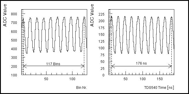
Qualitative demonstration of the performance of the DSC shows the response to a 50MHz Sine Wave (Fig. 5) where the raw ADC data of the DSC are compared to the digital scope output.

Fig. 5: Raw ADC Data of the DSC response to a 50 MHZ sinusoid (left) compared to the digital scope output (right). 117 bins in the DSC are 176ns, which corresponds to a sampling speed of 665MHz.
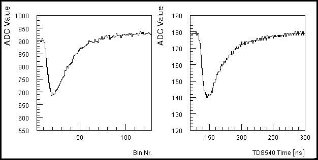
A pure CsI crystal viewed by an EMI 9821QB photo-multiplier was connected to the DSC test setup and data was taken with cosmic muons.
A typical CsI signal is shown in Fig. 6. The main parameters of the pulse are rise time, decay time and charge integral,
which agree with the result obtained from the digital scope TDS540.

Fig 6:Raw ADC data of the DSC response to a pure CsI pulse (left) compared to the digital scope output (right).
For future use in high multiplicity detector systems the read-out speed of the system is very important. Good results were obtained with the present system at 2MHz per bin, which corresponds to 64 musec for a 128-bin DSC.
In addition to a good signal reconstruction zero suppression is important: In the final detector system all the 240 CsI crystals are equipped with DSC's. Monte-Carlo simulations predict for a typical PIBETA event contributions from only ~5% of the CsI calorimeter. 95% of the modules will carry no significant pulse information, the DSC's belonging to these crystals will not be read out. A zero suppression circuit has been designed and implemented on the new iteration of the DSC.


