 DSC Test Environment
DSC Test Environment
DSC Test Environment
500 DSC are available for the PIBETA experiment now. Before building DSC modules we have to test the chips individually. Testing means, that we have to check, if the Readbit will be clocked through the shift register and if the sampling works recently. We operate a single DSC in a 'simple mode' and look if the Readbit will be clocked through the readout shift register and the signal output shows that a pulse on the input is sampled.
We've measured the response of the Zero Suppression. We measure the threshold voltage, when the Zero Suppression starts working for a DC offsetted pulse. Variation of the Domino Speed voltage should show a different output for a fixed signal. If these criteria are fulfilled, the chip is accepted and ready for motherboard production.
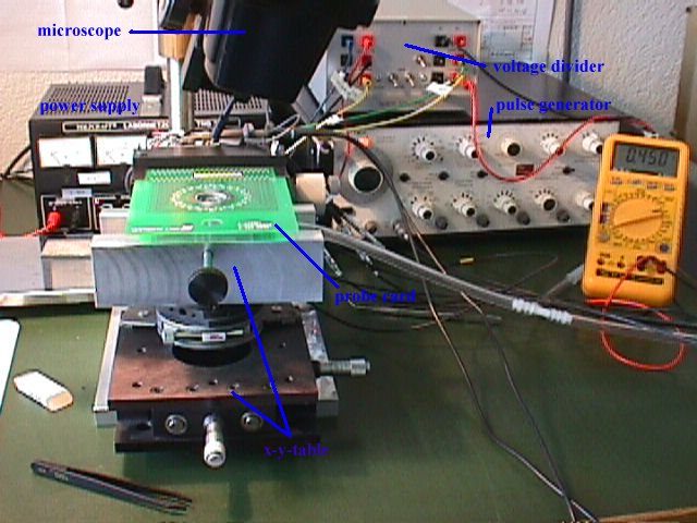 Figure 1: DSC Test Setup
The chips are on blocks of 6 each. This blocks are held by vacuum to keep them in a fixed position, without the use of glue. We have a cube of Plexiglas (figure 2) with 3 drains and a connection to a vacuum pump.
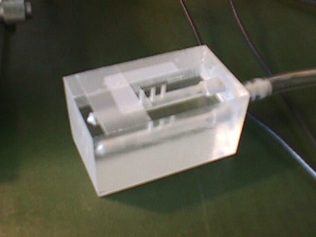 Figure 2: Plexiglas Cube
This block is mounted on a x-y-table to adjust the x-y position of the
chip relative to the probecard needles. The probecard is fixed on an independent
table, moveable in z-direction. When the chip is in its right position
one can move the card downward to contact the needles to the bondpads of
the chips. A stereo microscope is used to control the right positioning.
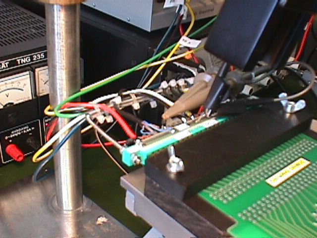 Figure 3: Probecard connections to power supply and sequencer
A full table of connections, used by the DSC in the test setup is given
here in table 1:
| Probe Pin | Pad # | Signal | Comment |
| 2 | 11 | V- dig | 1.3V-, Test 0V |
| 5 | 13 | Gate | CPG |
| 6 | 15 | RBI | CPG |
| 7 | 17 | Clear=Reset | CPG |
| 12 | 18 | Threshold | voltage divider, variable |
| 14 | 2 | GND ana | 0V, Test +1.2V 1/3 V+ |
| 18 | 4 | RBO | RBO Pin |
| 19 | 6 | Phi 1 | CPG |
| 24 | 9 | V + | 3.7 V + |
| A | 10 | V - dig | 1.3V-, Test 0V |
| AA | 8 | V + | 3.7 V + |
| D | 12 | V ds | voltage divider, variable |
| E | 14 | En ZS | voltage divider, switched |
| F | 16 | 3-pad | internal jumpered |
| N | 19 | Input | pulse generator |
| P | 1 | V add | last 4 cells not in Test |
| U | 3 | Output | Output Pin |
| V | 5 | ROR | internal jumpered |
| W | 7 | Phi 2 | CPG |
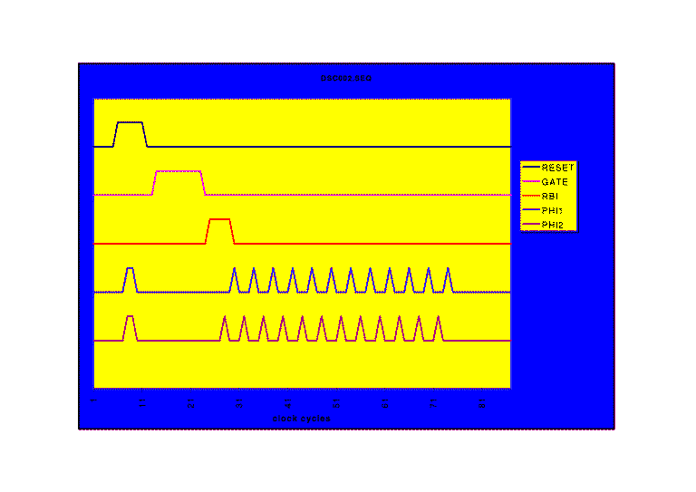
Figure 3: Example for a simple Control Sequence for the DSC
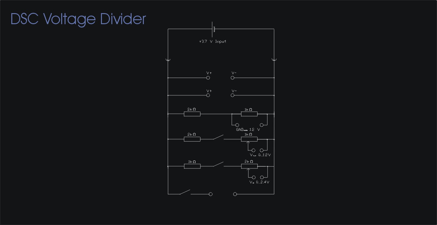
Figure 4: DSC Voltage Divider Circuit Diagram
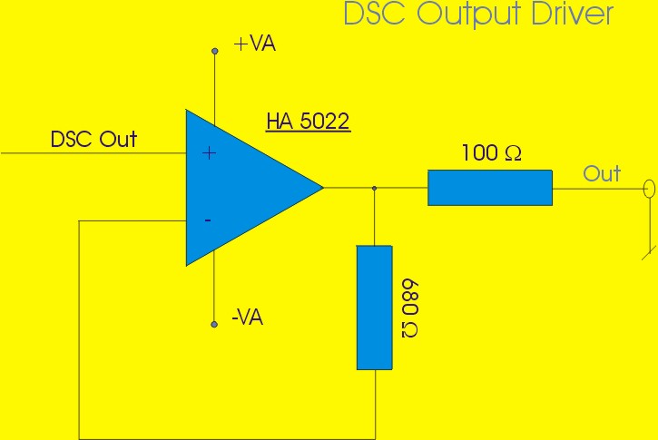
Figure 5: DSC Output Driver Circuit Diagram
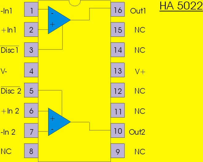
Figure 6: HA 5022 OpAmp pin connections. V+, V- = +/-5 V (symmetrically!!!)
.

H.P. Wirtz, Dec-1998
last update 09-Aug-2000