 DSC Simple Setup
DSC Simple Setup
DSC Simple Setup Here you will find some principal descriptions how to run the DSC in
your own simple setup or to help understanding the operation.
Here you will find some principal descriptions how to run the DSC in
your own simple setup or to help understanding the operation.
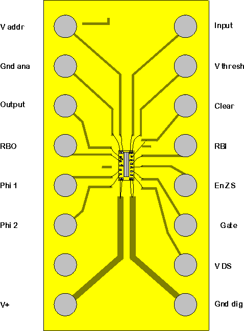
Figure 1: DSC simple carrier (made for the Novosibirsk group), also available as CDR file.
Signal optimization and termination has to be done externally.
![]()
| Pad # | Signal | Comment |
| 1 | V add | Address voltage |
| 2 | GND ana | Pibeta 0V,Test +1.2V 1/3 V+ |
| 3 | Output | Output Pin -> FADC |
| 4 | RBO | RBO Pin -> sequencer |
| 5 | ROR | internal jumpered, not used |
| 6 | Phi 1 | CPG |
| 7 | Phi 2 | CPG |
| 8 | V + | +3.7 V |
| 9 | V + | 3.7 V + |
| 10 | V - dig | Pibeta -1.3 V, Test 0V |
| 11 | V- dig | Pibeta -1.3V, Test 0V |
| 12 | V ds | connect to V + |
| 13 | Gate | CPG |
| 14 | En ZS | 0/1 TTL level |
| 15 | RBI | CPG |
| 16 | / | internal jumpered |
| 17 | Clear=Reset | CPG |
| 18 | Threshold | only if ZS enabled |
| 19 | Input | Signal Input |
Table 1: Operating voltages and signal connections
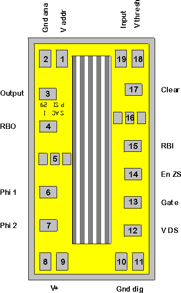
Figure 2: DSC pads, also available as CDR file
CPG stands here for 'Clocked Pattern Generator'. The sequencer can be realized by a clocked PLD. The DSC uses TTL logic for operation.
In our test setup the digital steering signals are produced by a 12 bit sequencer CPG 501,
externally clocked by 1 MHz. The
DSC requires TTL levels, but the CPG module gives just +2.6 V (logical
1) on 50 Ohms out. It is possible to operate the DSC with this minor
voltage by reducing the DC voltage V+ from 4.5 V to 3.7 V.
The necessary logical signals and the timing are shown in figure 3:
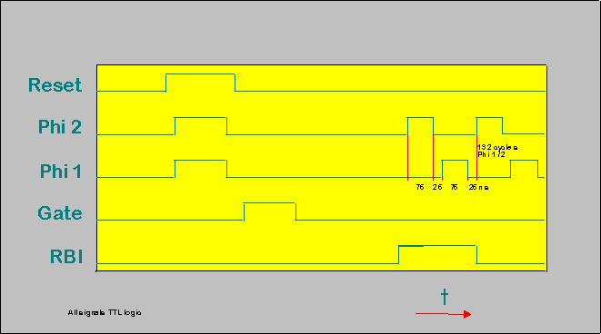
Figure 3: DSC operation sequence, also available as CDR file
![]()
.

H.P. Wirtz, last update 09-Aug-2000