
The operation of the DSC consists of the sampling phase and the readout phase. The principle of the sampling mechanism can be explained by a domino wave model: A logic pulse is transmitted through two sequential CMOS inverters and therefore reproduced; since the retardation of an inverter is ~500ps, the pulse is delayed by ~1ns. Thus a signal propagating through a long chain of inverters acts like a domino wave. The circuit diagram of the DSC is shown in Fig.1 :
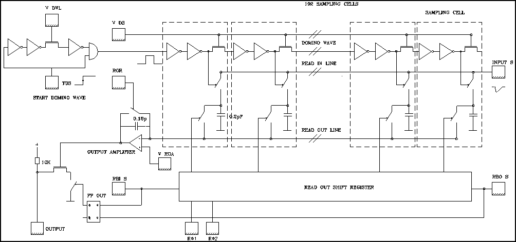
Fig.1: Circuit Diagram of the DSC.
A positive edge applied at the SDW (start domino wave) pad starts the domino wave which after every second inverter connects the read-in line with a storage capacitor; therefore the instantaneous level of the read-in line voltage is hold. The width of the domino wave is controlled by the domino wavelength voltage. The domino speed voltage V_DS influences the propagation time of the domino wave and therefore the sampling speed. In the present version, this mechanism works from ~0.4...~1.2 GHz, as shown in Fig. 2.
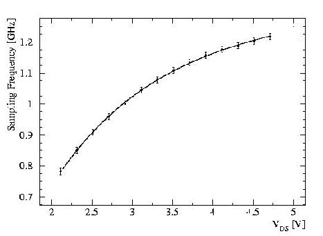
Fig.2: Sampling speed vs V_DS.
The input signal is DC coupled to the INPUT S pad. The read out of the stored information is done by applying four signals (see Fig.1): The RBI (read bit in) pulse, which is clocked through the read-out shift register with the signals Phi1, Phi2. A usual cyclus for the DSC is described here.

Ch. Broennimann, 6. Jan 1995
last update: H.P. Wirtz, 09-Aug-2000