


Clusters are combinations of several adjacent CsI crystals. GEANT simulations have shown clusters of about 7 crystals to be optimal in efficiency for determining showers above 55 MeV [Brö 96]. In the final detector, 60 overlapping clusters will be used. Clusters are formed using the UVa 125 summer/discriminator NIM style modules designed specifically for this task. The UVa 125 adds the voltages from up to 9 inputs. Since the modules do no integration of signals, it becomes imperative to have the input signals timed with one another as accurately as possible. The UVa 125 discriminates on the summed signal using two externally supplied thresholds.
Ten different superclusters are defined, each having two logic signals corresponding to the higher and lower discriminator thresholds in the UVa 125. The two discriminator outputs from a single cluster are input into two different LRS 4564 OR logic units. Signals from six different clusters are OR'ed together to create a supercluster signal. Two diametrically opposed supercluster signals must occur in a small time range (~20 ns) in order for a pion beta decay trigger to fire.
Each of the CsI crystals (except the few odd-shaped half-D and veto crystals surrounding the endcaps) is viewed by a 3" PhotoMultiplier Tube (PMT) manufactured by EMI Technologies (UK). The tubes are powered by bases designed and built at the University of Virginia. Each PMT signal is split at the base into two separate lines. One is delayed through about 75 m (385 ns) of PK-50-2-16 cable and will be referred to as the "analog leg". The PK-50-2-16 cable was manufactured in Siberia and was used because it was considerably less expensive than RG-58. The second line from the base feeds what will be referred to as the "trigger leg".
Once the cluster signals are formed, they are sent to an LRS 4564 OR logic CAMAC module where the superclusters are formed and logic is performed to output four signals.These four signals are p b HI, p b LO, p e n HI and [pi]e n LO. Since a partial array of only 44

Figure 3.14: Analog leg of the data acquisition electronics. Signals from all the detectors are split so that one part is digitized while the other part is used to create logic signals used by time to digital converters and scalers.

Figure 3.15: Trigger leg of the data acquisition electronics. One of the outputs from each phototube is split into four signals. Clusters are formed from analog additions of these signals while superclusters are formed from the logical ORing of cluster signals.
CsI crystals were used during the 1997 beam time, only one supercluster was available. Two supercluster signals SC0HI and SC0LO were used in place of p b HI and p b LO while the p e n HI and p e n LO inputs were left unconnected.
The SC0HI and SC0LO signals were sent through an LRS 4518 programmable delay unit along with several signals generated by beam line detectors that are described below. The LRS 4518 can be used to adjust the timing of each of its inputs before the signals are passed on to an LRS 2365 Octal Logic Matrix module. The LRS 2365 is a programmable logic module that will generate up to sixteen outputs, each made from a different logical combination of the sixteen inputs. A diagram showing the inputs and outputs of the LRS2365 used by the pibeta experiment can be seen in Figure 3.16. For the 1997 beam time, only eight of the outputs were used, each representing a trigger for a different event type.
The LRS 2365 output is sent to the input of an LRS 4516 logic unit where they are logically ANDed with eight signals from an IO 506 input/output CAMAC module. By writing a logical "false" to certain lines of the IO 506, certain trigger types can be "turned off" via the computer. A copy of the outputs of the LRS 4516 are eventually sent to an LRS 4448 coincidence register. The LRS 4448 coincidence register will latch the input lines during an externally supplied gate. This allows the bit pattern indicating which trigger types were valid for a specific event to be read out and recorded with the event. This feature has several very useful benefits. Besides making the experiment easier to maintain, this feature allows the accumulation of data of different types evenly over time. This is particularly beneficial
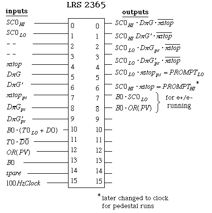
Figure 3.16: Inputs and outputs of the LRS 2365 module at the heart of the trigger electronics.
when using events of one trigger type to calibrate events of another trigger type. In the case of gain matching, the use of alternate "gain matching" and "pion decay" runs would mean the appropriate CsI gain matching factors would be accurately known only during times when no pion decay data were being taken. This can mean significant improvements in overall detector resolution if the gains tend to drift over time. Gain drifts in the 1997 data are discussed in the section on data analysis. Throughout the design of the trigger logic for the pion beta decay experiment, emphasis has been made on making the system configurable via computer. This means few, if any , changes should ever need to be made to the wiring once the initial setup is complete. Additionally, the trigger conditions will be stored automatically with each run reducing the chance for human error.
 ).
This signal is created when a pion is stopped in the target (T0). Created from
the logical AND of B0, D0, and T0HI. The T0 detector determined the
timing and was cut on a high threshold so as not to trigger on decay products
in the target
).
This signal is created when a pion is stopped in the target (T0). Created from
the logical AND of B0, D0, and T0HI. The T0 detector determined the
timing and was cut on a high threshold so as not to trigger on decay products
in the target* D p G The delayed pion gate is generated by the p stop signal but delayed by 10 ns to allow prompt events, such as pion scattering, to occur before looking for signals in the calorimeter. This pulse was 75 ns wide. A supercluster signal in coincidence with this signal will trigger the digitization electronics to begin recording values for all of the detectors * D p G' The delayed pion gate prime is generated by the D p G signal but delayed to start ~100ns after D p G starts. The D p G' captures events in which the calorimeter is hit long after most pions have decayed and so provides a good measurement of the Michel (i.e. p + -> µ+ n ) background. A supercluster signal in coincidence with this signal will trigger the digitization electronics to begin recording values for all of the detectors.
A timing diagram showing the relation of these signals can be seen in Figure 3.17.