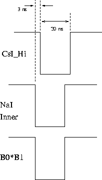
Figure 2.10: Reconstruction of the signals for the two arm trigger configuration
(CsI![]() NaI Inner
NaI Inner ![]() (B0
(B0![]() B1).
B1).
The two single arm triggers are comprised of the B0![]() B1 coincidence, and
one of either the CsI or NaI detectors. In this way, it is possible to detect
the photons from the single charge exchange reaction and the 129 MeV photon
from the pion capture reaction
B1 coincidence, and
one of either the CsI or NaI detectors. In this way, it is possible to detect
the photons from the single charge exchange reaction and the 129 MeV photon
from the pion capture reaction ![]() . Like the two arm trigger,
the thresholds for triggering the arrays are set as noted in
Sec. 2.2.5. The timing of each single arm trigger is determined
appropriately by the CsI and NaI arrays. The CsI single arm trigger configuration
is shown in Fig. 2.11.
. Like the two arm trigger,
the thresholds for triggering the arrays are set as noted in
Sec. 2.2.5. The timing of each single arm trigger is determined
appropriately by the CsI and NaI arrays. The CsI single arm trigger configuration
is shown in Fig. 2.11.
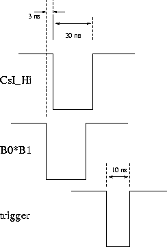
Figure 2.11: Reconstruction of the signals for the CsI one arm trigger
configuration (CsI![]() (B0
(B0![]() B1)).
B1)).
The rates for the single arm and two arm triggers depend on that of their components. These trigger component rates for the 116 MeV/c beam runs are summarized in Table 2.3. The schematic of the electronics used in the 1997 beam time are shown in Figs. 2.12 through 2.20.
Table 2.3: Experimental rates for 1997 Panofsky Ratio measurement.
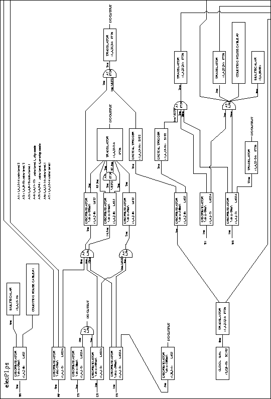
Figure 2.12: First of eight panels showing a schematic of the electronics used during
the 1997 beam time. Drawing courtesy of Michael Dugger, Arizona State
University.
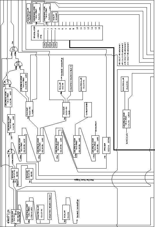
Figure 2.13: Second of eight panels showing a schematic of the electronics used during
the 1997 beam time. Drawing courtesy of Michael Dugger, Arizona State
University.
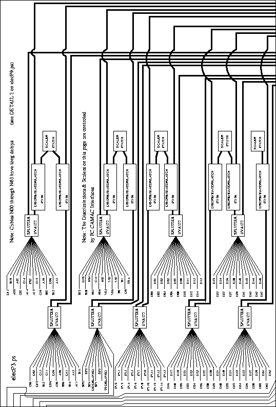
Figure 2.14: Third of eight panels showing a schematic of the electronics used during
the 1997 beam time. Drawing courtesy of Michael Dugger, Arizona State
University.
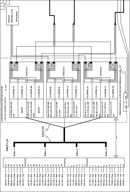
Figure 2.15: Fourth of eight panels showing a schematic of the electronics used during
the 1997 beam time. Drawing courtesy of Michael Dugger, Arizona State
University.
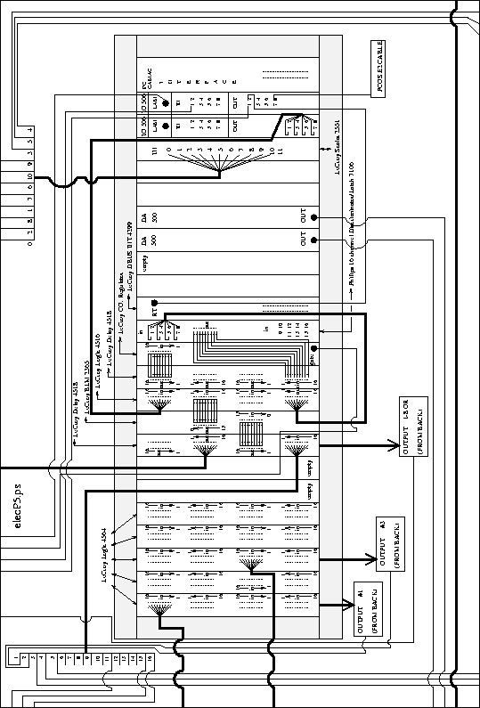
Figure 2.16: Fifth of eight panels showing a schematic of the electronics used during
the 1997 beam time. Drawing courtesy of Michael Dugger, Arizona State
University.
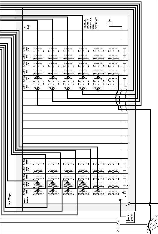
Figure 2.17: Sixth of eight panels showing a schematic of the electronics used during
the 1997 beam time. Drawing courtesy of Michael Dugger, Arizona State
University.
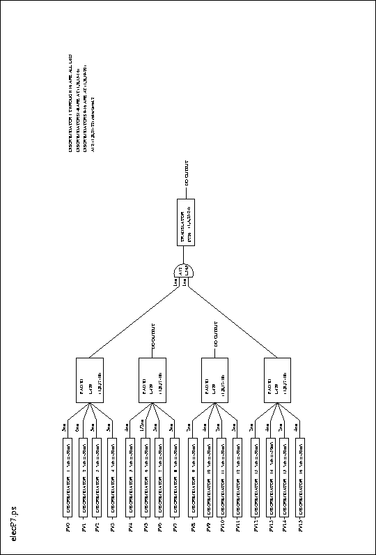
Figure 2.18: Seventh of eight panels showing a schematic of the electronics used during
the 1997 beam time. Drawing courtesy of Michael Dugger, Arizona State
University.
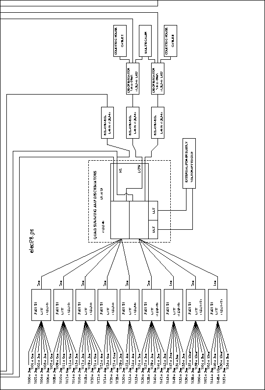
Figure 2.19: Eighth of eight panels showing a schematic of the electronics used during
the 1997 beam time. Drawing courtesy of Michael Dugger, Arizona State
University.
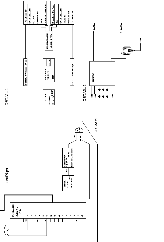
Figure 2.20: One of eight panels showing a schematic of the electronics used during
the 1997 beam time. Drawing courtesy of Michael Dugger, Arizona State
University.