


 (3.a),
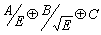
where
 indicates a squared sum. Here A is the noise term, B the stochastic term and C
the constant term. The optical non-uniformity directly contributes to C since
it can be interpreted in a similar way as a gain difference in neighbouring
crystals. Assuming a conical distribution of the electromagnetic shower with
depth r and defining f to represent the opening angle of
the shower cone, the integrated shower energy S is
indicates a squared sum. Here A is the noise term, B the stochastic term and C
the constant term. The optical non-uniformity directly contributes to C since
it can be interpreted in a similar way as a gain difference in neighbouring
crystals. Assuming a conical distribution of the electromagnetic shower with
depth r and defining f to represent the opening angle of
the shower cone, the integrated shower energy S is
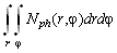
with Nph representing the distribution of photoelectrons/MeV within the calorimeter. Consequently the longitudinal and radial variation due to optical non-uniformity and gain variation s c is
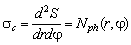
and thus s c/E = Nph/E=constant=C1.
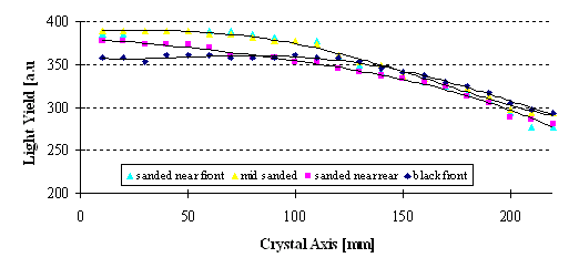
Tapered crystals are likely to have a position dependence in their light output. This started a series of investigation to minimize the influence of the non-uniformity without degradation of the light yield, which will be introduced in the following section. The required uniformity had to be better than 0.3%/cm for the first half of the crystal. (Since the shower mean of 70 MeV positrons or photons lies within the first third of the crystal length, the second half (nearby the read out) is of lesser importance.)
In order to overcome non-uniformity, a number of surface treatments of the front side and additionally a variation of reflecting materials has been investigated. The non-uniformity sufficiently was reduced by placing a black paper onto the front side, which still allows total reflection at this side due to an air gap, but which will absorb all the light leaving the crystal through the front face.
Since the reflectivity of the wrapping material is a function of wavelength several standard materials as PTFE[14]-Foil (Teflon), Millipore©, Tyvek© and aluminized Mylar have been tested. The first three materials are diffuse reflectors which mean that they obey the (2nd) Lambert law[15], while aluminized mylar acts as a mirror.
* Teflon, originally developed by DuPont, is an inert PTFE foam. The foaming process gives PTFE a white colour and hence good reflective properties. It is widely available in several thicknesses and sizes. For this test 50 µm thick PTFE-foil was used.
* Millipore Membranes are fabricated for the use in biological and chemical laboratories as filter sheets. They consist of polyvinylidene fluoride (PVDF) and are available in different varieties with a standard thickness of 110 µm. Their reflection properties have been investigated for some years [Bir93], but main disadvantage are the high costs.
* Tyvek, from DuPont, has the advantage of low cost at a good reflectivity. However, it is lacking opaqueness and normally has a thickness of 250 µm.
The development process was carried out in two stages. Firstly, two rectangular CsI crystals of the same manufacture as for our specific crystals have been wrapped with the same material at a time to account for systematic imperfections. An UV-sensitive PMT was coupled with an airgap to the crystals. Then the light yield was determined by the response to cosmic muons.
As a result of this test two materials were excluded from further examinations. From experience a diffuse reflector is better suited for a bulky and truncated scintillator [Der82,Bir93]. As expected, the wrapping with aluminized mylar showed the lowest light yield. Due to a low opaqueness and probably a low reflectivity in the UV-region the Tyvek wrapping did not lead to promising results. A treatment of Tyvek with reflecting paint (Kodak White Reflectance Coating 6080), which offers a reflectivity of more than 95% for UV light, could not improve the light yield notably. Also the use of painted Mylar was considered; but it was not applicable for wrapping any more after drying.
In the second step also the non-uniformity of the light output was measured. This was realized at a test set-up at the p [Mu]1 beam line at PSI with 80 MeV protons. A three inch EMI 9822QKB phototube has been coupled to the crystal using an adhesive silicon rubber (DowCorning 6500). The crystal to probe was put in a light tight and temperature controlled box that was located behind two quadratic wire chambers. By this the light yield and the point of incidence were obtained simultaneously. For this evaluation only the portion of light that was collected during the first 100 ns was taken into account.
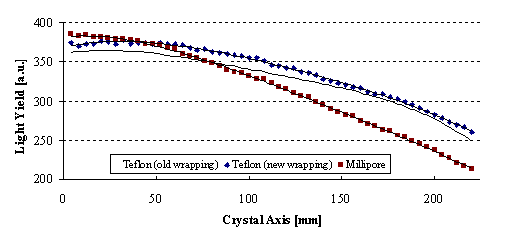
Different shapes of the CsI crystals have been used for the evaluation of the wrapping material to account for the geometric influence to the light collection. Two kinds of Durapore sheets and different wrapping thicknesses of Teflon have been investigated. After this, some methods to reduce optical non-uniformity have been compared (see Figure 3-8).
Two layers of properly wrapped Teflon-foil provided higher light output than one layer of Millipore, which had a comparable thickness. This was demonstrated for several crystals (one typical example is shown in Figure 3-7). Nevertheless, Bird et al.[Bir93] found Millipore to be superior to Teflon, since he obtained a better energy resolution for CsI(Tl) crystals. Although Millipore (in this study) showed better results for a sample of pure CsI with a large (>50%) contribution of the slow emission component, Teflon seems to have better reflecting properties for UV-light. This is decisive since pure CsI has the main emission component peaking at 310 nm.
As a result two layers of Teflon foil finally suited best the requirements of reflecting properties, optical uniformity and reasonable costs. Also a minimization of inactive material between the crystals was achieved this way. The Teflon layers were surrounded by one layer of aluminized mylar foil that both optically `seals' the crystal and protects the Teflon foil from dirt and damage.
In order to provide reproducibility a 2'' PMT (Philips XP2020Q) was permanently coupled to the test-crystal. After gluing the PMT to the crystal the coat was applied by dipping the crystal into the solvent that dried after a few hours. To avoid PMT damage the suggested `baking' of the lacquer was avoided; thus the coating did not stick perfectly onto the surface and could easily be removed for cross-checking. Nevertheless a uniform film of ~10 µm coating on the CsI could be applied that way. The light output of this crystal was measured with different wrapping materials, with and without coating using both cosmic muons and a pion beam. In either case the light output did slightly decrease after applying the coating. This idea of coating therefore was not followed any more until a Ukrainian group came up with a lacquer where a wavelengthshifter (WLS) was added to the coating material. So a set of crystals (one of each type) was chosen to demonstrate the properties of the lacquer. They were investigated in the RASTA apparatus (see ch. 3.3.4.3) for light yield, uniformity and timing before and after painting. In order to obtain the timing resolution the crystal was sitting between two 9.5 mm thick plastic scintillators. The signals from the plastic scintillator were used for the TDC start, which was stopped by the CsI signal. The standard deviation of the timing distribution then determined the timing resolution. Before and after painting the value was between 0.5 and 0.6 ns. So one could conclude that the WLS in the lacquer does not degrade the overall collecting time of light within the crystal. For the studied crystals an increase in light yield up to 30% has been established and, even more important, the uniformity improved considerably.
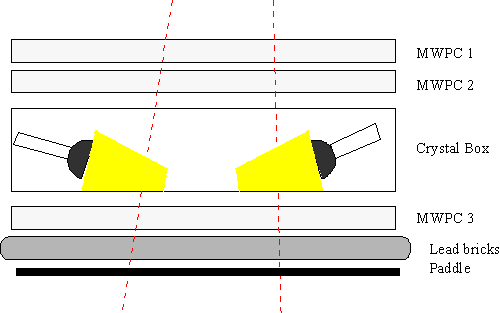
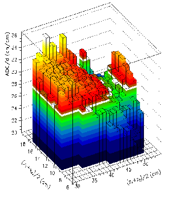
The cosmic ray tomography apparatus consisted of three drift chambers, two above and one below the crystals. For the trigger two plastic scintillators were positioned on the floor, separated from the lower drift chamber by 5 cm of lead bricks, to allow the selection of minimum ionizing cosmic particles. The drift chambers have two orthogonal x-y-planes surrounded by three ground plates. The chambers allow cuts on cosmic muons that penetrated the crystals almost vertically (>85 °). Hence, a correlation between the light output per unit pathlength and the position can be set up, which results in a mapping of the position dependence of the crystal's light output. A typical result can be seen in Figure 3-10.
A 137Cs source was mounted on a 5cm x 10cm x 20cm lead brick collimator with a 6 mm hole. A frame of 15 mm plywood was built to accommodate a CsI crystal with its PMT and to move the lead collimator on top of the crystal. Two PENT and one HEX C crystal were covered with a light tight cardboard enclosure of 2 mm thickness. The PMT and the voltage divider were the same as for the final set-up. While one output of the base was terminated, the other output was fed into an Ortec 454 timing amplifier with a gain of 30 and time constants of 50 ns for both integration and differentiation. The same signal was discriminated at 60 mV to produce a trigger. The signal was digitized with a peak sensing Ortec AD811 ADC and histogrammed. The source produced triggers at roughly 3kHz. Several background runs were taken without the source but with the lead brick and subtracted from the spectra that were obtained with source. It was found that the background spectra were not sensitive to the exact position of the lead brick. ADC pedestal runs were taken with a clock trigger and used to correct the spectra. During the measurements for one crystal, the temperature variation was less than 0.3 Kelvin.
After background subtraction, the spectra were fitted with a Gaussian function. In order to take account of the Compton edge of the 137Cs spectrum, an additional exponential background term was fitted. The centre and FWHM of a Gaussian distribution fitted to each spectrum was evaluated. The obtained centre then was corrected by subtracting the measured ADC pedestal. The statistical error at about 90000 counts was less than 0.3% for each source position. For each crystal, five points along the central axis were taken plus some points off-axis.
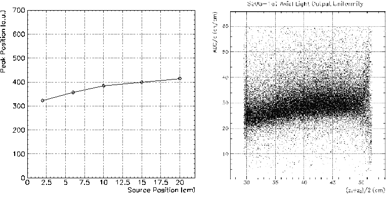
. Figure 3-11 shows the equivalence between the peak position of a 662 keV photon (left side) and the tomography result using cosmic muons. The FWHM of the source measurement increases near the PMT where the light output is highly non-uniform due to the optical geometry. As a conclusion, the uniformity results obtained with a 137Cs source are clearly correlated to the tomography data. Not only the general trend was reproduced, but also the quantitative uniformity obtained for the central axis was measured reliably. Since the photon energy of the 137Cs source is sufficient to penetrate on average several centimetres of CsI, not just the surface but the interior of the crystal was probed. As it was impossible to track individual photons, the edge regions of the CsI could not be probed.
Since it was found that this faster and simpler method is consistent with our 3D tomography and well suited for uniformity tests an automated measuring apparatus was designed. It was called RAdioactive Source Tomography Apparatus, abbreviated as RASTA. It relies on a PC to control a stepping motor, collect information for each position and analyze the data.

The 137Cs-source is embedded in a Pb-collimator with an opening of 6 mm diameter. It has a thickness of 5 cm; thus the probability to penetrate the lead is <1% for the 0.66 MeV photons. The collimator, which is mounted on a plate, can be moved by an ISEL stepping motor with a precision of ~12.5 microns (the crystal itself is can be placed with ~0.3 mm precision). An RS232 interface is used to control the stepping motor by PC.
[14] PolyTetraFlourEthylene
[15] If the rays meet the surface at an angle, then the illuminance is proportional to the cosine of this angle with the normal.