
The Domino Sampling Chip setup is a very fragile system. It might be
e.g. that there are very many address error messages about bad DSC
addresses after working on the ADCs. A 'wrong' touch to the input
cables to the DSC motherboards can be enough to screw up the whole
system.
In most cases it might be enough to take new address values, because
the touch of a cable may affect a small shift of the DSC baseline
which shifts all address values.
Start odbedit on pc2106 from the directory online. Change directory by
cd Equipment/Trigger/Settings/DSC
A typical odb-file from this directory is dsc_setup.odb. You can see the possible values. Usually the Address Lock is set to boolian y. This means that the address values are kept untouched. The Auto lock counter variable defines after how many events the Address get locked. So first of all one has to set all addresses to '0' by
set "Address Min[*]" 0
set "Address Max[*]" 0
In adition one has to switch the Address lock to n and set a value for the Auto lock counter e.g. to 100:
set "Address lock" n
set "Auto lock counter" 100
After you have started a run for every RANDOM Trigger event, where all DSC channels fire, the address values are taken and after 100 of these events the minimum value and the maximum values are stored in the odb and the Address Lock will be set to boolian y. If one sees that there is only a change necessary for an individual channel one can set the min or max value by hand with the same command and the proper value instead of the '0', e.g.
set "Address Min[48]" 3030
Error messages from the DSC e.g. about bad address values are written into an individual log-file dsc.log. Here one can lookup if an DSC Alarm has occured.
In The DSC Address EXCEL sheet one can see the data taken from one odb-file after taking address data, taken into excel for graphical visualisation and calculating e.g. address distances.
The most important tool to debug and setup the DSC system is the
standalone program DSC Test running on the Frontend PC. Before
you start the program make sure, that the Frontend is not
running. Start the b>DSC Test program by double clicking the Icon
with an IC and the name b>DSC Test on the desktop. It opens DOS
window and a menu shows up. The first two modes are only for very
special debugging purposes. In mode 3 all chips are read
out. This mode one should only use if the Zero Suppression is
switched off (all chips are firing!). This can be selected by a jumper
on the Controller. This mode can be used e.g. to set the
address values by the potentiometers on the carriers.
In Mode 4 an address to channel relation will be calculated by a
function. This mode is usable if e.g. a single channel is missing and
Mode 5 is not usable therefore.
In Mode 5 the program waits for a testpulse where all
channels fire. Then it accumulates the address to channel data (actual
value, min. max.; data get always updated). This mode is important to
see if the system is working and to set the correct Zero
Supression thresholds. After starting the program with a normal
production or Cosmic trigger with Random events the address values
should be collected within a few seconds. Then one can see that the
address values in the upper block are always firing for different
channels. The upper and lower bounds for the addresses can be seen in
the next two blocks. One can check if the addresses are correct and
that they are not overlapping.
One indication that something is running bad with the DSC system are the LEDs on the trigger and clock inputs of the FADC in the VME crate. In the past I have seen, that the clock LED is still on while the Trigger LED goes on and off. Whenever they are running asynchronous it is an indication for a more complicated problem. First of all one has to find out which motherboard induces the problem. This can easiest be done by unplugging them on the backside bus one by one and look after the standalone program ist started, if the Clock and FADC Trigger LEDs blink synchronous. It might be that it works again after unplugging the bus cable on the backside and replugging it. Sometimes you have to do it a few times (unplugging and replugging), but often this helps.
It might be that a DSC goes bust. The easy way is, if you are not able to fix a problem by the unplugging and replugging, then you should maybe replace carrier by carrier on the bad DSC motherboard, plug it back to the system and look how it behaves in the DSC Test Program. If this also doesn't help, exchange the motherboard. The bad motherboard also as the bad carrier has to be investigated for repair. The carrier can be tested by the test setup in the lab. A bad motherboard can be brought to Peter Dick from the Electronics Pool. If a DSC on a carrier has be exchanged, Silvan Streuli from the Horisberger Group can take a bad DSC off by a dentists drill. Then you have to glue a new DSC onto the carrier board.
There are 7 complete spare carriers (they are all tested!). and in addition 7 DSC chips from the same series and in addition about 1000 DSC from another series. These chips are all on blocks of 6 DSC together with 2 cips from another experiment. They have to be cutted and tested, as descibed on the DSC Test Page.
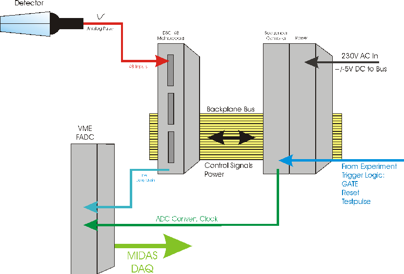
The main part of the DSC Sequencer is an Altera epm7032s FPGA which
produces all control signals from the input signals.
The Controller and the necessary signals are described on theController Page
Details on the necessary control sequences you can find on the DSC Homepage.
.

H.P. Wirtz, last update 09-Aug-2000